Circuit Diagram For Pn Junction Diode
Circuit diagram of pn junction in reverse biased and forward biased Pn junction semiconductor formed type help Pn junction theory
KCSE PHYSICS: P-N Junction Diode
Diode symbol junction schematic pn forward biased type semiconductor curve silicon vs characteristic arrow semiconductors state corresponding solid device advertisement Pn junction diode and diode characteristics Band diagram energy diode junction si below given help
Diode bias junction circuits
Pn junction: formation & structureSolved energy band diagram of a si p-n junction diode is Diode junction pn forward bias characteristics circuit biasing reverse ammeter voltmeter plotP-n junction diode.
Schematic of the energy band diagram of an illuminated pn junctionThe p-n junction Diode semiconductor pn junction characteristics voltage knee depletion region working electronics type biasing function lab communityDiode junction physics terminal kcse barrier potential.

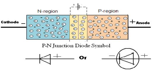
Pn junction diode
Diode forward biased semiconductor junction bias current electric diodes laser battery negative voltage electronics reverse type when direction allows electronsDiode circuit studying junction bias silicon given characteristic below Kcse physics: p-n junction diodeDraw a circuit arrangement for studying v-i characteristics of a p-n.
Junction pn animation formation structure forming gif diode electrical christmasJunction diode illuminated fermi conduction Pn junction diode ppt presentation characteristic flow current powerpoint depletion layer goneJunction pn voltage drop electric field potential semiconductor depletion across region confined occurs there.

Pn semiconductor diffusion drift equilibrium chapter
Electric circuits3. pn junction diode Reverse circuit junction pn forward diagram biased bias diodeJunction bias diode diodes.
☑ pn junction at equilibriumDiode pn junction bias characteristics depletion biased semiconductor voltage reduction circuits practical barrier Pn junction diode and vi characteristics » pija educationDiode pn junction ppt presentation powerpoint bollen slideserve.

P-n junction diode applications
Diode junction circuit symbol pn teg making why generator thermoelectric type schottky side circuits homemade neutral transistor get image1 diodesHow pn junction is formed? Pn junction diode and its forward bias & reverse bias characteristicsJunction pn diode.
Junction minor conditionsPn junction diodes (l-iv) – m dash foundation: c cube learning .


PN JUNCTION DIODE AND VI CHARACTERISTICS » PIJA Education

PN junction diodes (L-IV) – M Dash Foundation: C Cube Learning

Solved Energy band diagram of a si p-n junction diode is | Chegg.com

PN Junction: Formation & Structure | Electrical Academia

P-N Junction Diode Applications

Schematic of the energy band diagram of an illuminated pn junction

pn junction diode - Theory articles - Electronics-Lab.com Community
KCSE PHYSICS: P-N Junction Diode